Heidelberg team 3D-prints plug for fiber-to-chip photonic coupling with sub-dB loss
Heidelberg researchers 3D‑printed a Two‑Photon Polymerization plug with total‑internal‑reflection micro‑optics that achieves sub‑dB fiber‑to‑chip coupling across 1500 to 1600 nm and packs in under three minutes per port.
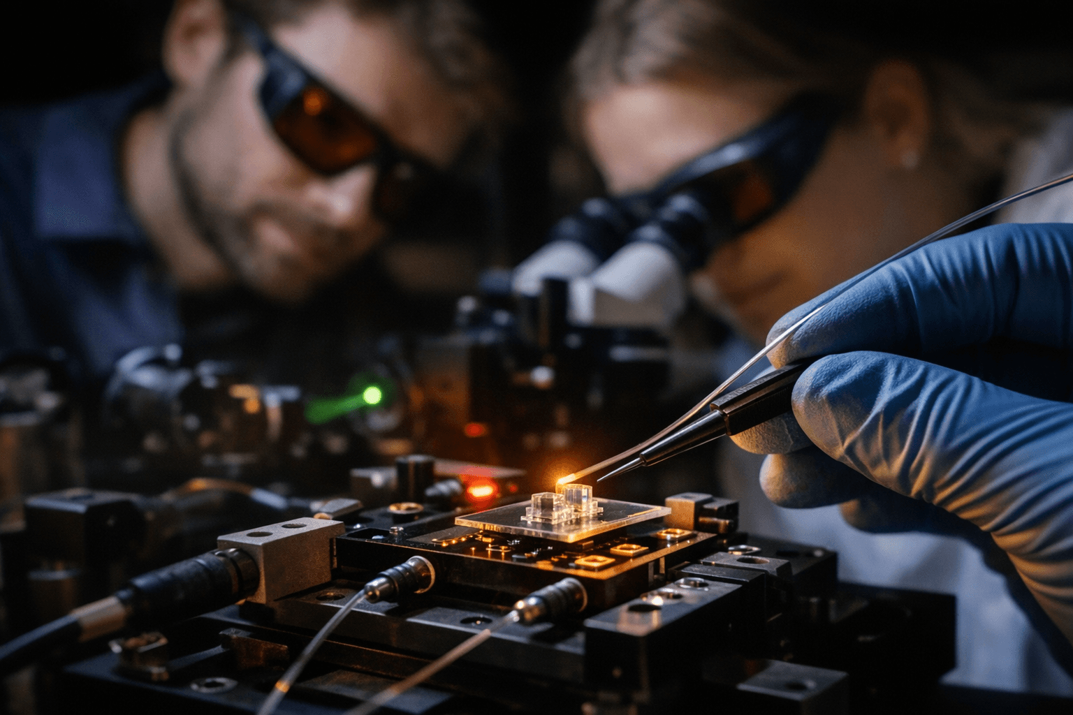
Prof. Wolfram Pernice’s group at the Kirchhoff Institute for Physics, Heidelberg University, and doctoral researcher Erik Jung demonstrated a plug‑and‑play fiber‑to‑photonic‑chip connector produced by aligned high‑precision 3D microprinting that delivers sub‑dB insertion loss across telecommunications wavelengths 1500 to 1600 nm and requires under three minutes packaging time per port. The device is reported in a peer‑reviewed paper listed under DOI 10.1126/sciadv.adz1883 with E. Jung and W. Pernice among the authors.
The printed component integrates three‑dimensionally printed total internal reflection couplers with a passive mechanical micro‑optical interlock fabricated directly on the photonic chip. The interlock is designed to mate with standardized multi‑fiber termination push‑on arrays (MTP) using the MTP’s alignment pinholes, producing a self‑aligned, insertion‑locked connection that removes the need for active, micrometer‑scale alignment and microlens fabrication, according to Heidelberg University materials describing the work.
Performance details cited by the team include broadband, wavelength‑independent transmission between 1500 and 1600 nm and repeated claims of sub‑dB coupling loss; the press material and technology transfer listings do not give a single numeric insertion‑loss figure beyond the sub‑dB descriptor. The researchers demonstrated the approach on a neuromorphic photonic processor described variously in source materials as a 16‑input‑port photonic tensor core and as a device with 17 ports; the differing port counts appear in the University release and in industry summaries respectively. Erik Jung stated, "This 'plug and play solution' guarantees that no data is lost in the course of the coupling process."
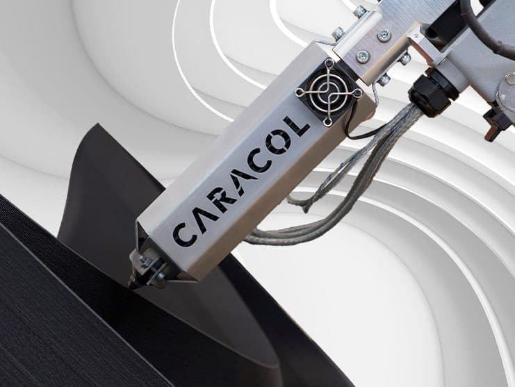
Fabrication used aligned Two‑Photon Polymerization (2PP) microprinting directly onto the chip facet to create TIR couplers that redirect and focus waveguide modes into fiber cores. Technology transfer copy notes that combining different 3D printing techniques enables sub‑micrometer positioning of fiber array patch cables, and Nanoscribe imagery referenced by the authors illustrates ultra‑compact 3D splitters consistent with the micro‑optics approach.
The project involved collaborators from the Institute for Molecular Systems Engineering and Advanced Materials and formed part of the "3D Matter Made to Order" Cluster of Excellence at Heidelberg University. The team lists co‑authors H. Gehring, F. Brückerhoff‑Plückelmann, L. Krämer, C. Vazquez‑Martel, and E. Blasco alongside Jung and Pernice. ScienceValue’s technology transfer entry identifies the development stage as Prototype, marks the IP as patent pending, and indicates the group is seeking a licensee; ScienceValue Heidelberg GmbH can be contacted at Berliner Straße 47, 69120 Heidelberg, phone +49 (0)6221‑567435, email ScienceValue‑Heidelberg@med.uni‑heidelberg.de. Heidelberg University’s main switchboard is listed as +49 6221 54‑0.
If the sub‑dB claims and durability hold up under the detailed measurements and lifetime testing reported in the full paper, the printed plug concept could materially lower the time and cost barriers that have long constrained scalable photonic integrated circuit packaging and enable modular, reconfigurable PIC deployments in neuromorphic computing and communications.
Know something we missed? Have a correction or additional information?
Submit a Tip