TSMC unveils A13, N2U chips, signals gains without costly ASML tools
TSMC said it can keep shrinking and speeding up chips while leaning on existing EUV tools, a move that could slow demand for ASML’s costliest machines.
TSMC used its annual technology symposium in Santa Clara to send a clear message to the chip industry: the next round of gains may come from extracting more out of existing manufacturing tools, not from rushing to the newest and most expensive ones.
At the 2026 North America Technology Symposium on April 22, the company unveiled A13, a direct shrink of its A14 node, and N2U, a lower-cost process option aimed at phones, laptops, AI systems and high-performance computing. TSMC said A13 is scheduled for production in 2029, delivers 6% area savings versus A14, and remains fully backward compatible with A14 design rules. N2U is set for production in 2028 and is designed to offer 3% to 4% speed gains or 8% to 10% lower power, along with a 1.02x to 1.03x logic-density improvement versus N2P.
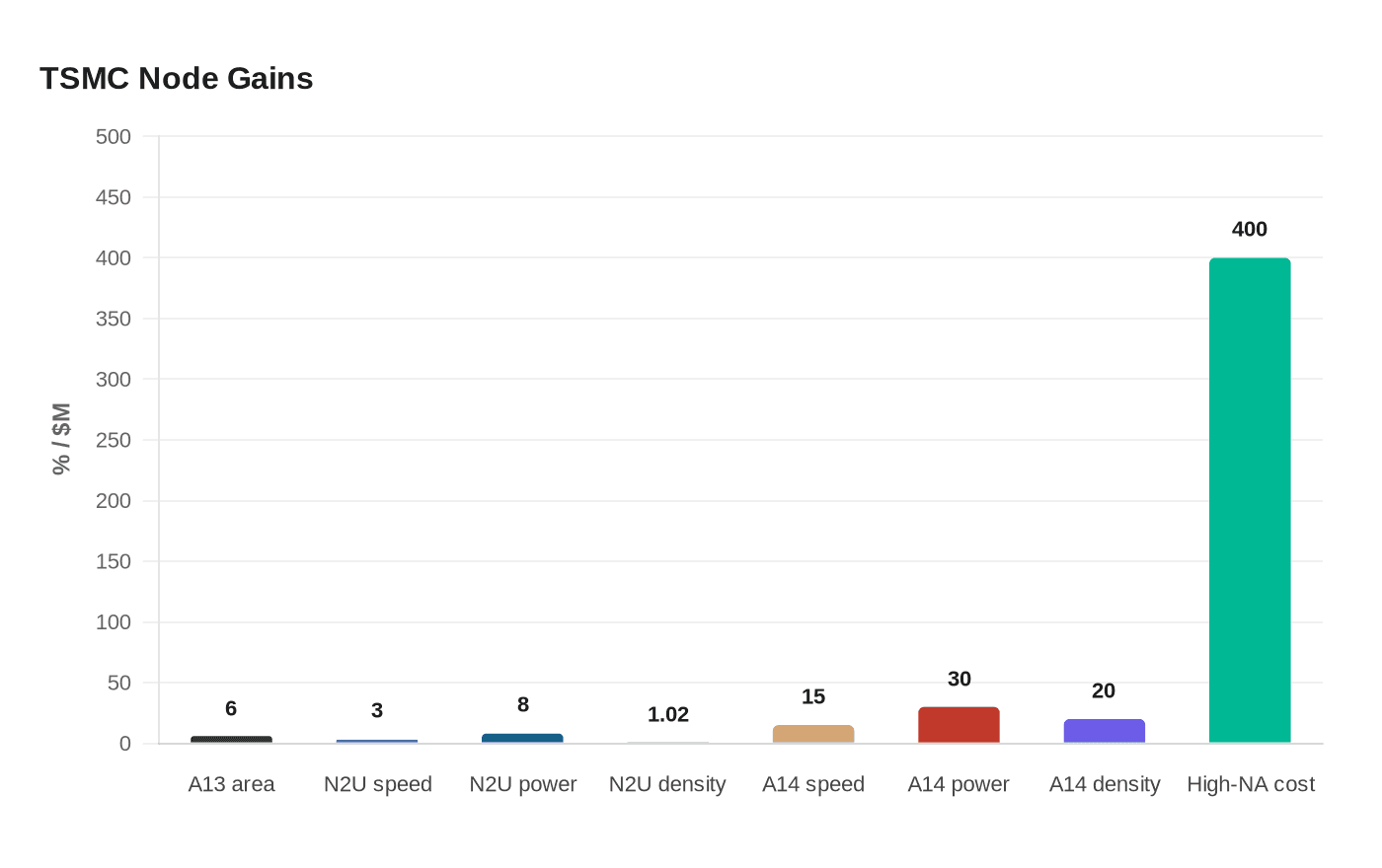
The pitch matters because it suggests TSMC believes it can keep improving performance without immediately moving wholesale to ASML’s high-NA extreme-ultraviolet tools, which can cost about $400 million apiece. For the world’s most advanced foundry, that is more than a product update. It is a signal about capital discipline in an industry where every new node can reshape supply chains, pricing power and competitive advantage.
TSMC chairman and chief executive C.C. Wei said the company aims to provide customers with a “reliable stream” of new silicon technologies and described TSMC as their most reliable technological partner. Kevin Zhang said the company’s research and development has done exceptionally well in leveraging existing EUV technology while setting an aggressive scaling roadmap. That message positions TSMC’s current equipment base as capable of carrying more of the load, at least for now.
TSMC also previewed A12, an enhancement to its A14 platform that uses Super Power Rail backside power delivery for AI and HPC applications. A12 is scheduled to enter production in 2029. The company framed the lineup under the theme “Expanding AI with Leadership Silicon,” underscoring how closely its roadmap is tied to the surging demand for AI accelerators.
The timing builds on last year’s symposium, when TSMC introduced A14 and said it was planned for production in 2028. That node was expected to improve speed by up to 15% at the same power, or cut power by up to 30% at the same speed, while delivering more than 20% higher logic density. Together, A14, A13, N2U and A12 show a company pushing multiple levers at once: smaller transistors, better power delivery and more efficient packaging.
For Nvidia, Apple and Google, the announcement reinforces TSMC’s central role in advanced chipmaking. For ASML, it hints that near-term demand for high-NA tools may be slower than once expected. More broadly, TSMC is arguing that cutting-edge semiconductor progress can still be capital-efficient, even if the bottleneck is shifting from raw lithography to how much performance can be squeezed out of the tools already in the fabs.
This article was produced by Prism’s automated news system from verified source data, official records, and press releases, then run through automated quality and moderation checks before publishing. The system is built and supervised by the people who set the standards it runs under. Read our full AI policy.
Did this article answer your question?