New pretreatment could make chip etching safer and more precise
A simple oxygen or fluorine pretreatment cut the energy to strip sulfur from MoS2 to as low as 10 eV, a possible fix for a key chipmaking bottleneck.

A small chemistry change may help decide whether atom-thin chips stay a lab curiosity or become a manufacturing platform for faster, cooler hardware. Researchers at Princeton Plasma Physics Laboratory said coating molybdenum disulfide with oxygen or fluorine before plasma processing made it far easier to remove only the top layer of sulfur atoms, a step that could tighten control over etching in next-generation semiconductors.
That matters because the commercial question is not whether ultrathin materials can do impressive things in a paper. It is whether chipmakers can manufacture them reliably, at scale, without wrecking the layers underneath. Silicon is edging against its physical limits, and the push for smaller, more energy-efficient devices has turned transition metal dichalcogenides, or TMDs, into a serious candidate for future computing, sensing and quantum hardware.
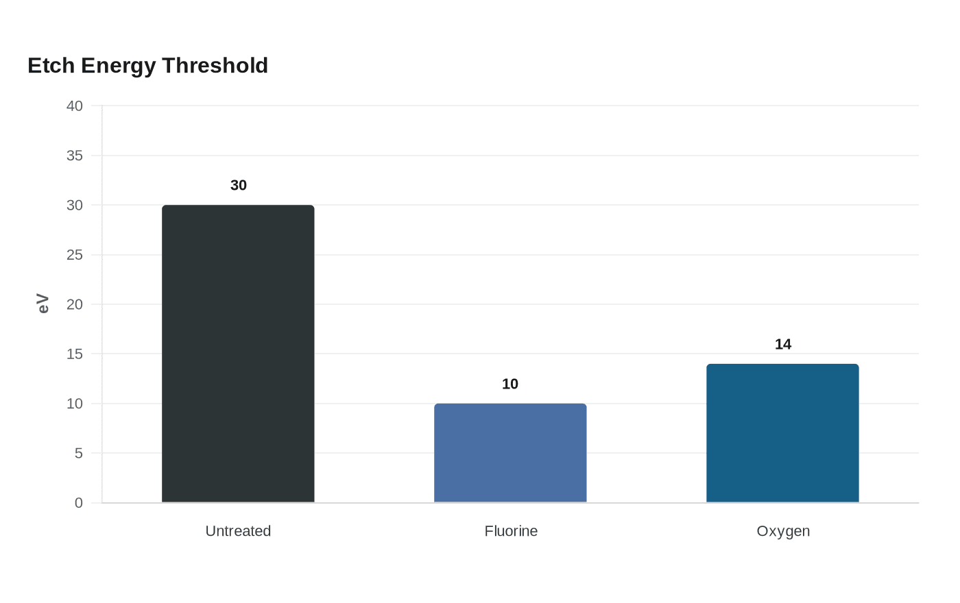
The Princeton team said the pretreatment lowered the energy needed to knock a sulfur atom loose from about 30 electron volts on an untreated MoS2 surface to about 10 electron volts with fluorine and about 14 electron volts with oxygen. That wider processing window could make selective chalcogen removal more precise while preserving the metal lattice below, which is exactly the kind of control semiconductor fabrication demands.
MoS2 is only three atoms thick, with one molybdenum layer sandwiched between two sulfur layers, so even tiny errors can alter device behavior. The study, published in the Journal of Physical Chemistry Letters, showed that surface chemistry can help plasma do finer work instead of blasting through a material that is already only a few atoms deep.
The team’s computer simulations also showed that oxygen and fluorine functionalization can form sputtering products such as sulfur dioxide and sulfur fluorides, helping carry away the top-layer sulfur without damaging what lies beneath. Scientists including Yury Polyachenko, Rachel Kremen and Mao were part of the work, which was reported in Princeton and broader science releases on June 16 and June 17, 2026.
The timing is significant for the United States, where advanced semiconductor manufacturing has become a strategic race tied to national security, supply-chain resilience and the next wave of energy-efficient computing. A better etch could help turn atomically thin materials into real products, instead of leaving them stranded in the lab.
That commercial pressure is already visible. In June 2026, other researchers reported a MoS2-based computer with more than 1,000 transistors on a single chip, a sign that 2D materials are moving closer to integrated devices. The bottleneck now is less about proving possibility than proving repeatable production, and this pretreatment points directly at that problem.
This article was produced by Prism’s automated news system from verified source data, official records, and press releases, then run through automated quality and moderation checks before publishing. The system is built and supervised by the people who set the standards it runs under. Read our full AI policy.
Did this article answer your question?