IBM Patent Targets 3D Printed Hollow Cavities as Functional Engineered Structures
IBM's patent WO2026058093 proposes turning 3D printed hollow cavities into functional structures by depositing particles that tune stiffness, heat transfer, and damping.
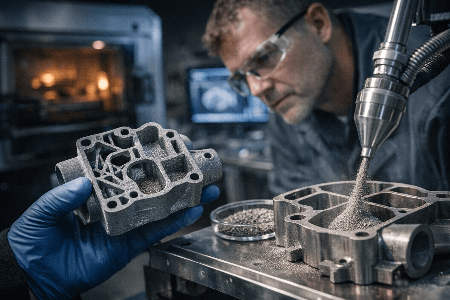
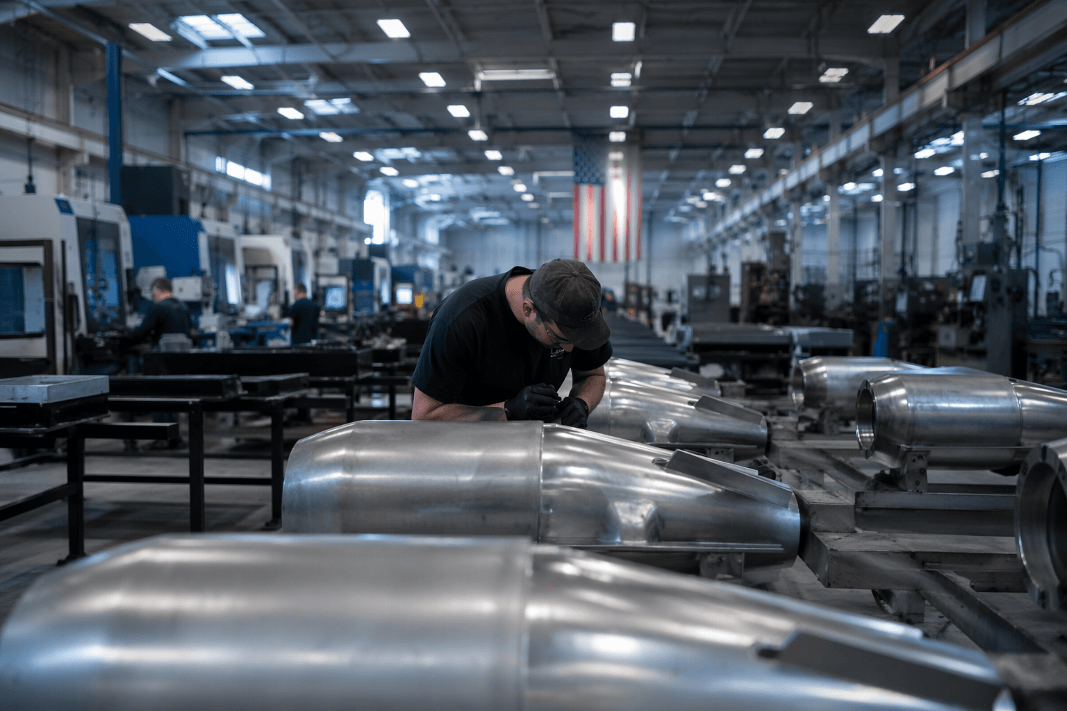
IBM filed a patent that reframes one of additive manufacturing's oldest assumptions: that hollow cavities are simply empty space. Published under WIPO number WO2026058093 and covered by Fabbaloo on March 26, 2026, the filing describes a technique IBM calls "hollow fill additive manufacturing," a method for depositing particles, sacrificial media, or engineered micro-features inside voids that would otherwise remain inert air.
At the core of the approach is solidification pattern recognition. IBM's abstract describes "identifying a solidification pattern for an object with a first hollow portion being created by a primary nozzle on an additive manufacturing device during a hollow fill additive manufacturing process." Rather than letting that hollow portion sit empty, the system selectively fills it with material chosen to alter specific properties: density, stiffness, thermal conductivity, or fluidic behavior.
The practical implications cut across several areas that experimental makers are already pushing into. A printed drone arm could be hollowed for weight savings but internally structured to preserve stiffness. A robotic actuator housing could carry a particulate mix tuned for vibration suppression. Internal channels designed for liquid cooling or conformal inserts become not just a geometric possibility but an engineered outcome with measurable, controlled performance characteristics.
None of this is shipping in a slicer today. IBM's filing is exploratory, and the gap between a WIPO application and a practical toolpath in PrusaSlicer or OrcaSlicer is significant. Converting the approach into usable tools requires slicer support, hardware capable of reliably depositing specialized infill agents, and safe material handling for any non-standard particles or resins involved.
What WO2026058093 does signal is a shift in how major technology players think about infill strategy. The standard sparse honeycomb or gyroid has long been the ceiling for most hobbyist workflows; IBM's filing treats interior geometry as a design variable rather than a necessary compromise. For slicer developers and materials companies watching the IP landscape, it marks a direction worth tracking closely. The patent won't unlock these capabilities on its own, but it confirms the R&D appetite is there.
This article was produced by Prism’s automated news system from verified source data, official records, and press releases, then run through automated quality and moderation checks before publishing. The system is built and supervised by the people who set the standards it runs under. Read our full AI policy.
Did this article answer your question?