Hot electrons enable 3D nanoprinting of metals at the nanoscale
Confined hot electrons can fuse metal nanocrystals into 3D shapes, a step toward chip, sensor and photonic manufacturing at dimensions conventional tools miss.
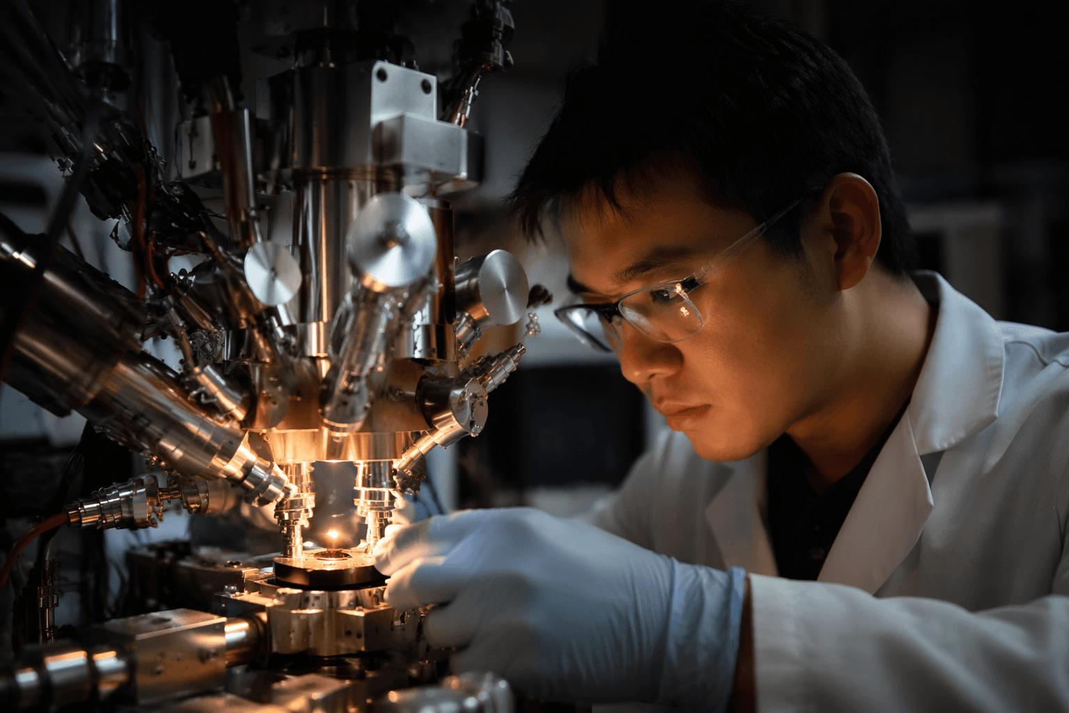
A burst of femtosecond laser light can now do more than heat a metal surface. In a Nature Communications study, hot electrons confined inside nanocrystals trigger multi-electron absorption, strip surface ligands and fuse metal building blocks into 3D structures at the nanoscale. The payoff is not just smaller printing, but a new way to shape metal where conventional manufacturing loses control over geometry.
How the process works
The paper was received on December 9, 2025, accepted on June 15, 2026, and posted on June 27, 2026. Its central idea is to turn transient electron excitation into a fabrication tool: femtosecond laser pulses generate hot electrons in nanocrystals, and those electrons stay confined long enough in space and time to drive the chemistry and bonding needed for printing.
The sequence is not simple thermal melting. It includes nonlinear multi-electron absorption, ligand desorption and nanocrystal fusion, which gives the method a more localized and selective mode of action than bulk heating.
Why the manufacturing payoff matters
The main industrial promise is precision at a scale where today’s tools struggle. The precision of 3D printing with inorganic materials is still limited, and that limitation becomes more severe as the target shrinks into the nanometer range. A method that can guide metal formation through spatiotemporally confined hot electrons addresses exactly that bottleneck.
At the nanoscale, tiny changes in shape can dramatically alter optical response, electrical transport and sensing performance, so the ability to build metal structures with finer spatial control opens a path to devices that are difficult to engineer by conventional means. The most obvious applications sit in chips, sensors, medical devices, optics and photonic materials, where intricate metal features can determine how light, charge or chemical signals move.
The manufacturing question is whether this can create structures that are not merely smaller, but more functional. If the method can be controlled reliably, it could make narrow gaps, sharp edges, stacked features and other complex 3D geometries more feasible than with standard deposition or lithography alone.
Why hot electrons are attractive as a fabrication tool
Hot electrons are already a well-studied phenomenon in plasmonic structures. Hot-electron generation offers high efficiency, broadband tunability and a high density of electrons concentrated in a well-defined volume near a metal surface. Those traits make them appealing wherever researchers want energy delivered fast, locally and with spectral control.
Instead of relying only on heat, pressure or chemical deposition, researchers can use electronically driven processes to steer matter into useful forms. In this study, that means the electron burst itself becomes the active ingredient that enables fusion at the nanocrystal level.
How this builds on earlier nanoprinting work
The 2026 paper does not arrive in isolation. A 2023 Nature Communications study, Metal 3D nanoprinting with coupled fields, showed that 3D metal nanostructures could be characterized through electron energy-loss spectra, with Auger electron microscopy used to analyze their electron excitations. That earlier work established that coupled fields could steer metal nanoprinting and that the resulting structures could be probed in detail after formation.
The new method pushes the field one step further by shifting emphasis from external field coupling to the transient physics of hot electrons inside nanocrystals. The difference is that the newer approach uses the excited electronic state itself as the engine of fabrication.
What still stands between the lab and industry
The remaining hurdle is not whether the physics exists, but whether it can be turned into repeatable production. Proof-of-concept demonstrations are valuable because they show that the mechanism works, yet industrial use demands throughput, uniformity and reproducibility across larger areas and more material systems. The same features that make the method powerful, ultrafast excitation and tight spatial confinement, also make it difficult to scale outside a carefully tuned optical setup.
That is where the precision limit in inorganic 3D printing becomes a commercial issue rather than just a scientific one. If the process cannot hold its shape control from one build to the next, it will remain a niche lab technique even if the underlying physics is elegant. The near-term challenge is to preserve the hot-electron advantage while adapting it to manufacturable workflows, so the field can move from writing a few nanoscale structures to building useful metal architectures with device-grade reliability.
This article was produced by Prism’s automated news system from verified source data, official records, and press releases, then run through automated quality and moderation checks before publishing. The system is built and supervised by the people who set the standards it runs under. Read our full AI policy.
Did this article answer your question?