Nvidia to unveil Rubin inference chips and shift Blackwell capacity
Nvidia will use GTC to roll out Vera Rubin inference hardware and shift production from H200 Blackwell, promising up to 5x inference and 10x lower token costs.

Nvidia plans to use its GTC developer conference in mid‑March to roll out a new generation of inference processors and to shift manufacturing emphasis from the H200 Blackwell family to the newly unveiled NVIDIA Vera Rubin platform, industry reporting said on March 6. The move, if sustained, reorients the company’s factory capacity toward lower‑latency, token‑economical workloads that are driving commercial demand for generative and agentic AI.
Nvidia first showed Rubin at CES 2026 and has begun publishing technical claims and system configurations. Jensen Huang, Nvidia’s founder and chief executive, framed Rubin as a timely response to rising AI demand, saying, "Rubin arrives at exactly the right moment, as AI computing demand for both training and inference is going through the roof." At CES Huang added, "Vera Rubin arrives just in time for the next frontier of AI" and, in remarks reported by a wire service, "I can tell you that Vera Rubin is in full production."
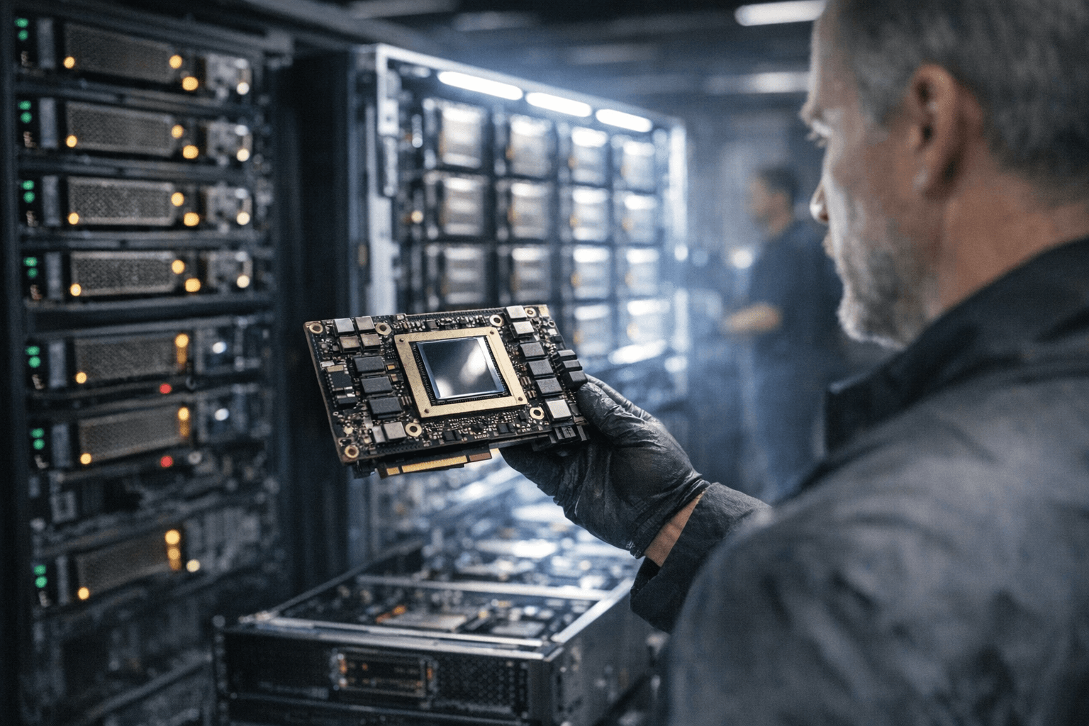
The Rubin platform is presented as a rack‑scale system and an HGX server option. Nvidia’s NVL72 rack combines 72 Rubin GPUs with 36 Vera CPUs, NVLink 6 fabric, ConnectX‑9 SuperNICs and BlueField‑4 DPUs. The company claims the NVL72 will deliver 3.6 exaFLOPS of NVFP4 inference and 2.5 exaFLOPS of NVFP4 training, with 54 TB of LPDDR5X CPU memory and roughly 20.7 TB of HBM4 across the rack at 1.6 PB/s of bandwidth. The HGX Rubin NVL8 links eight Rubin GPUs through NVLink for x86‑based generative AI platforms.
Nvidia and trade coverage published a catalogue of per‑GPU claims for the Rubin GPU: roughly 50 petaflops of low‑precision FP4 inference, 35 petaflops of FP4 training, eight HBM4 stacks totaling about 288 GB and 22 TB/s of HBM4 bandwidth per GPU, plus 3.6 TB/s of NVLink bandwidth. The company says Rubin delivers up to 5x inference performance and 3.5x training performance versus its Blackwell generation, and promises up to 10x lower cost per token for massive‑scale inference and the ability to train mixture‑of‑experts models with four times fewer GPUs.
Rubin’s architecture rests on what Nvidia calls an extreme six‑chip codesign: the Vera CPU, Rubin GPU, NVLink 6 switch, ConnectX‑9 SuperNIC, BlueField‑4 DPU and Spectrum‑6 Ethernet switch. The platform introduces an Inference Context Memory Storage tier using BlueField‑4 DPUs to share and reuse key‑value cache state across racks, a feature Nvidia positions as necessary as context windows grow to millions of tokens.
Some technical details vary by source. Trade outlets and Nvidia developer documents use slightly different spellings for the new low‑precision format, NVFP4 and NVPF4, while HPCWire and developer materials differ on memory multipliers: HPCWire cites a 2.8× HBM4 bandwidth improvement over Blackwell, while Nvidia developer text says Vera delivers 2.4× higher memory bandwidth and 3× greater memory capacity. Those discrepancies underscore lingering questions about baseline models and measurement methodology; industry reporting also cited a planned production shift away from the H200 Blackwell family.
The capacity move matters to cloud providers, AI startups and data center operators because inference economics govern per‑user latency and operating cost. Nvidia’s assertion that Rubin is already "in full production" and will ship "later this year" signals the company intends rapid supply and broad deployment. The change signals a clear strategic bet: optimize fabs and supply chains around token‑efficient inference hardware rather than concentrating solely on raw training throughput. If Rubin’s claims hold up in independent benchmarks, the industry will see pressure to adapt infrastructure and procurement toward racks optimized for long, multi‑turn agentic workloads.
This article was produced by Prism’s automated news system from verified source data, official records, and press releases, then run through automated quality and moderation checks before publishing. The system is built and supervised by the people who set the standards it runs under. Read our full AI policy.
Know something we missed? Have a correction or additional information?
Submit a Tip