Focused microwaves enable 3D-printed electronics on delicate materials
Focused microwaves now let printed electronics cure on leaf-thin, temperature-sensitive surfaces without cooking them, opening a path to wearable, biomedical, and embedded devices.
A print that stays gentle while the ink hardens
The real breakthrough here is not that electronics can be printed. It is that they can be printed and annealed on fragile surfaces that normally would not survive the process. Yong Lin Kong and his Rice University team use focused microwaves to heat conductive inks in place, while leaving the surrounding substrate relatively cool, which removes the bottleneck that has held back electronics 3D printing for more than a decade.
That changes the shape of the whole workflow. Instead of treating delicate materials as something to attach electronics to later, the process makes the electronics part of the print from the start. The result is a desktop-size route to freeform, multimaterial devices on temperature-sensitive materials that would usually be damaged by conventional thermal processing.
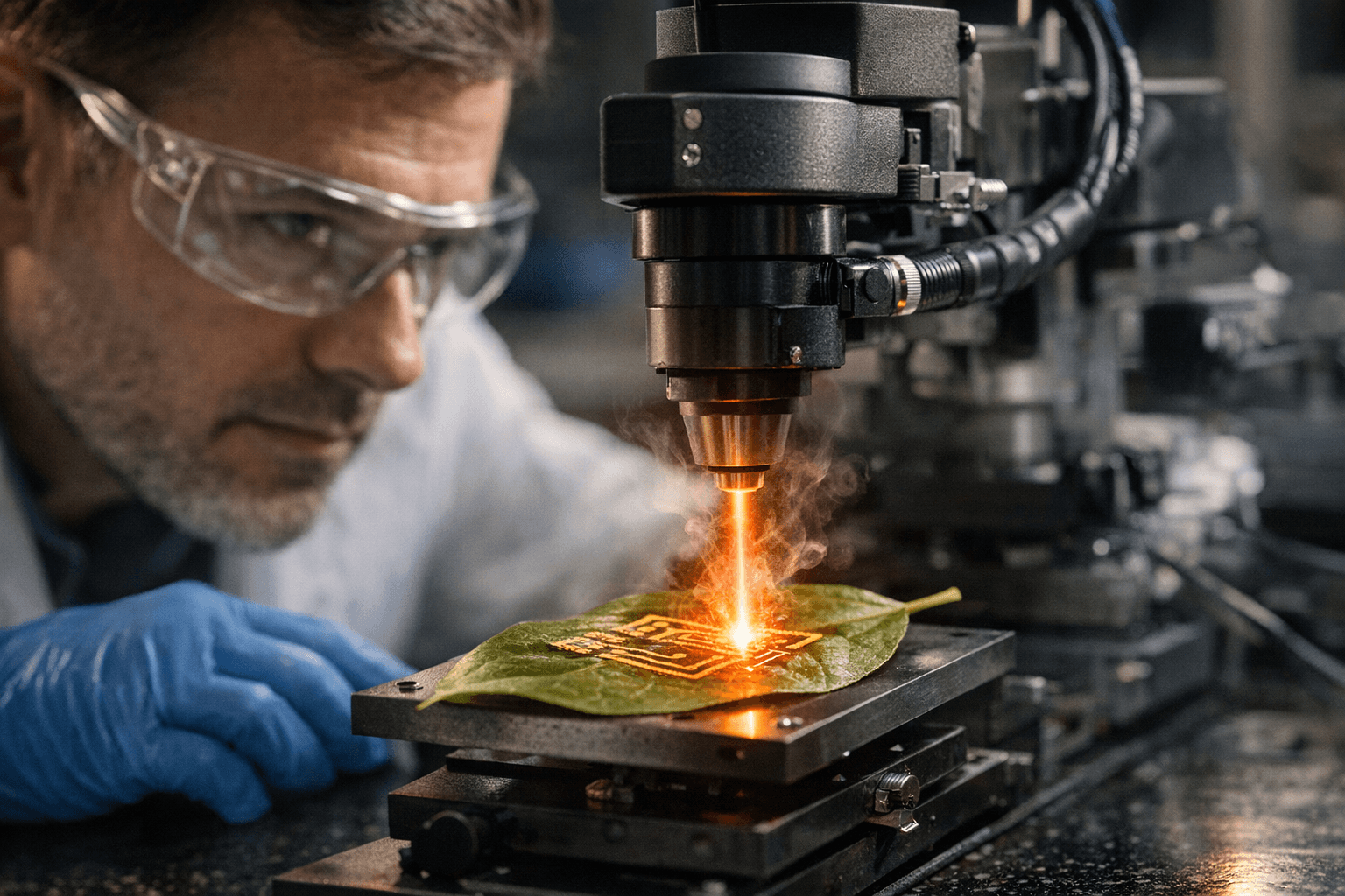
How Meta-NFS focuses the heat
At the center of the method is a metamaterial-inspired near-field electromagnetic structure, shortened to Meta-NFS. In plain terms, it concentrates microwave energy into a tiny zone, as small as the diameter of a human hair, so the ink receives rapid volumetric heating right where it is needed. That selective heating is the key move: the printed nanomaterials and polymers are treated in situ instead of being exposed to a blanket bake that could warp, scorch, or kill the substrate underneath.
The Science Advances paper describes this as a way to overcome the inability to selectively anneal printed materials on temperature-sensitive substrates. That detail matters because annealing is where many printed conductors become useful, but it has also been the step that made delicate substrates off-limits. By reshaping the energy field itself, the Rice team turns a thermal problem into a spatial one.
What the team demonstrated
The paper does not stop at theory. It shows a freestanding silver microarchitecture with a 30-micrometer trace diameter printed on a leaf, a demo that instantly tells you how controlled the process is. A leaf is about as unforgiving a testbed as you can imagine for electronics fabrication, and the fact that the structure survives there signals just how localized the heating becomes.
The researchers also printed on silicone to show high-resolution features on another temperature-sensitive material. That combination of leaf-scale delicacy and silicone feature work gives the technique a broader identity than a one-off lab trick. It looks like a manufacturing platform that can move across substrates, rather than a single-material novelty.
Rice says the process can integrate freeform electronics on biopolymers and living biological tissue in a desktop-size printer, without complex facilities or labor-intensive manual assembly. The paper also notes compatibility with optically opaque materials, which is a subtle but important point. If the system can work without needing light to penetrate the substrate, it becomes far more versatile for multimaterial builds where visibility and transparency are not guaranteed.
Why the material palette matters
The biggest story is not just that the prints are smaller or cleaner. It is that the material palette gets wider. The paper argues that broadening the set of printable substrates could enable classes of electronics that are hard to create any other way, including multifunctional circuitry with locally programmed electrical and mechanical properties.
That is where the future applications start to get interesting. Once you can print and cure conductors without wrecking the host material, the door opens to electronics embedded in places that once seemed impossible: biopolymers, bone, soft robots, and even ingestible devices. These are not just exotic surfaces. They are environments where flexibility, biocompatibility, and low thermal stress are the difference between a usable device and a failed prototype.
For the 3D printing community, that means embedded electronics stops being a separate post-processing problem and starts becoming part of the print architecture. Instead of adding wires after the fact, you can imagine routing conductivity through the structure itself, building sensors into curved shells, or placing functional traces inside soft, deformable parts without collapsing the part during curing.
What this signals for embedded builds, wearables, and multimaterial printers
For anyone already working in embedded electronics, wearables, or multimaterial printing, the lesson is straightforward: process control is moving from the nozzle to the energy field. A printer that can deposit material and then selectively anneal only the conductive path changes what counts as a viable substrate. That makes soft robotics more realistic, because compliant parts no longer have to withstand a brutal thermal step. It also points toward wearables that sit closer to skin, tissue, or flexible bio-based materials.
The desktop-size setup matters just as much as the chemistry. Rice’s framing suggests this is not limited to a specialized cleanroom pipeline. If the method can stay compact and practical, makers and labs could think in terms of hybrid electronic devices assembled with the same kind of flexibility that already drives multimaterial printing, but with much less damage risk to the host structure.
A shift from novelty to capability
This work, led by Yong Lin Kong and co-authors Jian Teng, Samuel H. Hales, Xin Yang, Jared Anklam, Saebom Lee, Yu Liu, Dwipak Prasad Sahu, Leibin Li, Cordelia Latham, Xi Tian, Derrick Wong, Taylor E. Greenwood, and John S. Ho, reads like a capability leap rather than a one-off headline. The technique was published in Science Advances, and its focus is practical: make printed electronics compatible with delicate, irregular, and temperature-sensitive materials.
TechXplore highlights the biomedical and robotics potential, and that is exactly where the method feels most consequential. If focused microwaves can keep the substrate cool while the ink gets the heat it needs, then the field gets to rethink where electronics can live. That is a much bigger change than simply printing another circuit, because it turns fragile surfaces into real manufacturing targets instead of off-limits exceptions.
This article was produced by Prism’s automated news system from verified source data, official records, and press releases, then run through automated quality and moderation checks before publishing. The system is built and supervised by the people who set the standards it runs under. Read our full AI policy.
Did this article answer your question?